EETimes – All Processing Bends Toward AI –

“I brought this up because we began thinking about using this for place-and-route in ASIC design,” Dean said. “The game of place-and-route is far bigger than the game of go. The problem size is larger, though there isn’t as clear goal as there is with go.”

Google created a learning model for place-and-route, and then set out to find if the tool could generalize. Could it take what it learned on one design and apply it to a new design it had never seen before? The answer was an unambiguous “yes.”

Furthermore, Dean said, “We’ve gotten super-human results on all the blocks we’ve tried so far. It does a little bit better, and sometimes significantly better than humans.”

Source: EETimes – All Processing Bends Toward AI –

Samsung Kicks Off Mass Production of AI Chip for Baidu: 260 TOPS at 150 W

Samsung Foundry and Baidu this week said that the companies were about to start mass production of an AI accelerator chip early in 2020. Baidu’s Kunlun chip is to be made using Samsung’s proven 14 nm process technology, and make use of the company’s Interposer-Cube 2.5D packaging structure.

Source: Samsung Kicks Off Mass Production of AI Chip for Baidu: 260 TOPS at 150 W

Apple and GPU-maker Imagination make nice in new licensing deal

Apple discusses the iPad Pro’s A12X CPU and GPU on stage at its October 30, 2018 event. (credit: Valentina Palladino) Imagination Technologies, which used to provide the graphics processors for Apple’s mobile devices, has entered into a new licensing agreement with Apple that comes after two years of turmoil between the companies.

Source: Apple and GPU-maker Imagination make nice in new licensing deal

Early TSMC 5nm Test Chip Yields 80%, HVM Coming in H1 2020

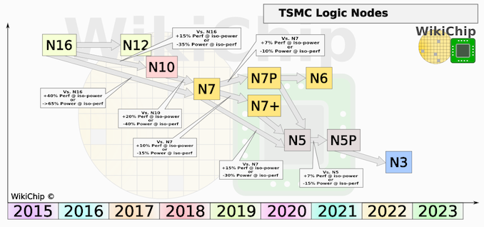
If you’re only here to read the key numbers, then here they are. In the disclosure, TSMC is stating that their 5nm EUV process affords an overall with a ~1.84x logic density increase, a 15% power gain, or a 30% power reduction. The current test chip, with 256 Mb of SRAM and some logic, is yielding 80% on average and 90%+ in peak, although scaled back to the size of a modern mobile chip, the yield is a lot lower. The technology is currently in risk production, with high volume production scheduled for the first half of 2020. This means that chips built on 5nm should be ready in the latter half of 2020.

Source: Early TSMC 5nm Test Chip Yields 80%, HVM Coming in H1 2020

Intel vs AMD vs Google vs Amazon vs NUVIA – Semiwiki

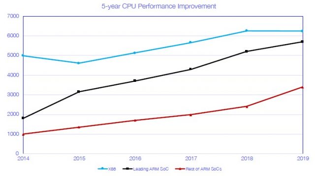
Google started it with their Tensor chip in 2016 (now in its third generation) followed by the Edge TPU in 2018. Last year Amazon announced their own Graviton chip which is based on the ARM architecture (now in its second generation). In fact, the only cloud companies of the top five (Microsoft, Amazon, Google, IBM, Oracle) that are NOT making their own chips are IBM and Oracle. IBM sold their semiconductor division to Globalfoundries in 2015 and Oracle recently abandoned the SUN Microsystems IC team they acquired in 2010 for $5.6B, ouch.


Source: Intel vs AMD vs Google vs Amazon vs NUVIA – Semiwiki